pcb design rules for digital circuit
PCB Placement and Routing - Mentor Graphics. 9 Images about PCB Placement and Routing - Mentor Graphics : Pin by A L on Projects to Try | Electronics rules, Circuit board design, PCB Design Terminology You Should Know | Tempo and also Pin by A L on Projects to Try | Electronics rules, Circuit board design.
PCB Placement And Routing - Mentor Graphics
 www.mentor.com
routing assisted xpedition
Layout Automation Using Advanced PCB Design Techniques - Part 1 | PADS
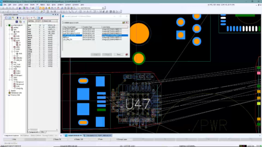 blogs.sw.siemens.com
reuse
How To Select The Best Printed Circuit Board Material For Your Design
 www.tempoautomation.com
pcb ground circuit material printed altium planes layer frequency select selection solidworks plane practices shortcuts layout grid substrate rf
(Yet Another) PCB Layout Without Schematic Question - Layout - KiCad
 forum.kicad.info
kicad schematic
Siemens PCB Schematic Design | PADS Professional | Cadlog
 www.cadlog.com
hyperlynx circuit schematic cadlog 機能 electronic
PCB Design Terminology You Should Know | Tempo
 www.tempoautomation.com
pcb terminology
PCB Design Engineer Resume Samples | QwikResume
 www.qwikresume.com
engineer qwikresume
Circuit Board Wallpapers - Wallpaper Cave
 wallpapercave.com
circuit wallpapers desktop computer backgrounds pc printed electronic 1280 pcb background 1024 electronics definition 1080p android wallpapersafari electronique wallpapercave pixel
Pin By A L On Projects To Try | Electronics Rules, Circuit Board Design
 www.pinterest.com
Layout automation using advanced pcb design techniques. Pcb design engineer resume samples. How to select the best printed circuit board material for your design